TPS22964CYZPR
- Description
- 5.5-V, 3-A, 14-mΩ load switch with output discharge 6-DSBGA -40 to 85
- Fault Protection
- Reverse Current
- Max Output Current
- 3A
- Turn-Off Delay Time
- 2.5µs
- Turn-On Delay Time
- 928µs
- Datasheet
Quantity
21,000 AvailableLet us do the sourcing. Even if it's not available now, our team can track it down and tailor a solution just for you.
- 3A Maximum Output current, Single High-Side Channel
- 1V to 5.5V Input and Supply Voltage Range
- Reverse Current Fault Protection with Output Discharge
- 928us Turn-on Delay and 2.5us Turn-Off Delay
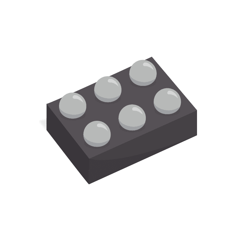
- 6-Ball DSBGA Chip-Scale package, 1.5mm X 0.9mm X 0.5mm
- -40C to 85C Operating range, 125C Maximum Junction Temperature
The TPS22964CYZPR is a Texas Instruments high-side load switch with output discharge and reverse current protection, rated for 3A of output current. It operates over a 1V to 5.5V input and supply range with an on/off control interface, a 928us turn-on delay and a 2.5us turn-off delay. The TPS22964CYZPR is supplied in a 6-ball DSBGA package measuring 1.5mm x 0.9mm x 0.5mm, rated from -40C to 85C with a 125C maximum junction temperature.
Load switches let a host cut power to individual subsystems, sequence rails at start-up, and eliminate leakage from blocks that are idle, which directly extends battery life in portable products. The controlled turn-on delay limits inrush current into capacitive loads so the upstream rail does not sag or trip its own protection, and reverse current protection stops a charged downstream node from back-feeding the supply. The 1.5mm x 0.9mm chip-scale package makes the TPS22964CYZPR a fit for smartphones, tablets, wearables, cameras and SSDs where board area is the binding constraint.
Fusion’s in-house quality hubs and Prosemi testing facility are fully certified to meet critical industry standards for electronic component inspection and testing.
Quantity
21,000 AvailableLet us do the sourcing. Even if it's not available now, our team can track it down and tailor a solution just for you.