LFXP2-17E-5FTN256I
- Description
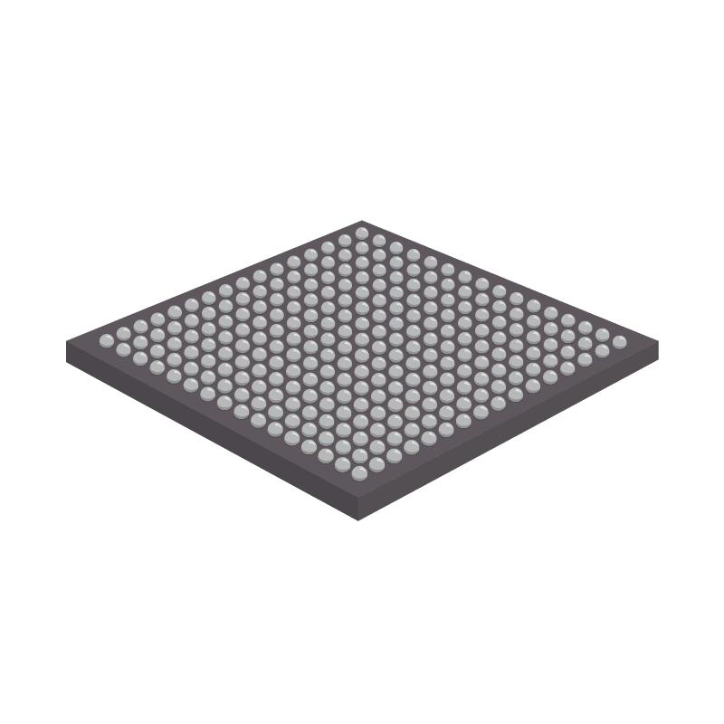
- FPGA LatticeXP2 Family 17000 Cells 90nm Technology 1.2V 256-Pin FTBGA Tray
- Number of I/Os
- 201
- Number of Logic Elements/Cells
- 17000
- RAM Size
- 34.5kB
- Datasheet
Quantity
Let us do the sourcing. Even if it's not available now, our team can track it down and tailor a solution just for you.
- 17000 Logic Elements for Complex Designs
- Operating Supply Voltage: 1.2V
- Max Supply Voltage: 1.26V
- RAM Size: 34.5kB
- Number of I/Os: 201
- Lead Free and RoHS Compliant
The Lattice Semiconductor FPGA LatticeXP2 Family is a versatile Field Programmable Gate Array designed for high-performance applications. With 17000 logic cells and built on advanced 90nm technology, this FPGA offers exceptional flexibility and efficiency for a wide range of digital designs. It operates at a nominal supply voltage of 1.2V and is packaged in a 256-pin FTBGA configuration, making it suitable for space-constrained environments. The device supports a broad temperature range from -40°C to 100°C, ensuring reliable performance in various operating conditions.
The FPGA LatticeXP2 Family is designed for a variety of applications, including digital signal processing, telecommunications, and control systems. It features 17000 logic cells and supports high-speed I/O interfacing, making it ideal for complex, resource-intensive designs. Engineers and developers in embedded systems often use this FPGA for custom hardware acceleration and prototyping.
Fusion’s in-house quality hubs and Prosemi testing facility are fully certified to meet critical industry standards for electronic component inspection and testing.
Quantity
Let us do the sourcing. Even if it's not available now, our team can track it down and tailor a solution just for you.