RC19004AGNL#KB0
- Description
- PCIe Gen7 4-Output Clock Buffer
- Max Output Frequency
- 156.25MHz
- Datasheet
Quantity
7,500 AvailableLet us do the sourcing. Even if it's not available now, our team can track it down and tailor a solution just for you.
- Four-Output Clock Buffer with HCSL and LVDS Output Types
- Output Frequencies Up to 156.25 Megahertz
- SMBus Configuration Interface
- Input Supply Range of 2.97V to 3.63V
- Operating Temperature Range of -40°C to 105°C
- 28-Pin 4mm by 4mm package, 900µm height, 400µm Pitch
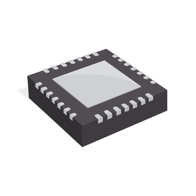
The Renesas RC19004AGNL#KB0 is a four-output clock buffer supplied in a 28-pin surface-mount package measuring 4mm by 4mm, with a 900µm height and a 400µm pitch. It supports output frequencies up to 156.25 megahertz with HCSL and LVDS output types and is configured over an SMBus interface. The RC19004AGNL#KB0 operates from a 2.97V to 3.63V input supply across a -40°C to 105°C temperature range. It is RoHS and China RoHS compliant, ships 2500 per reel, and Renesas lists its manufacturer lifecycle status as Active.
A clock buffer takes one reference clock and fans it out as several matched copies with low added jitter, so every receiver on a board sees the same timing without loading the source oscillator. HCSL and LVDS outputs at up to 156.25 megahertz are the standard signalling levels for serial-link reference clocks, so parts of this type are placed on server motherboards, add-in cards, switch and storage backplanes, and instrumentation boards. SMBus control lets platform firmware handle per-output enable and configuration instead of strapping resistors. Typical buyers are platform hardware engineers and ODMs building high-speed serial systems.
Fusion’s in-house quality hubs and Prosemi testing facility are fully certified to meet critical industry standards for electronic component inspection and testing.
Quantity
7,500 AvailableLet us do the sourcing. Even if it's not available now, our team can track it down and tailor a solution just for you.